FPGA Design
FPGA design overview:
The main design features of the FPGA is to receive digital audio from the external ADC, apply digital filters to the audio based on user inputs passed from the MCU, and then send the filtered audio to the MCU. The FPGA receives audio from the ADC using an I2S Communication Protocol, and next implements the onboard multiply-accumulator block (MAC) to the data and then outputs it. Due to time constraints, we were not able to implement digital filtering on our hardware, but we were able to get the desired behavior in ModelSim using the MAC.
Reading in Audio
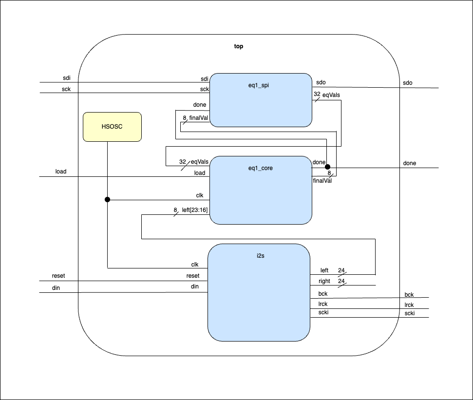
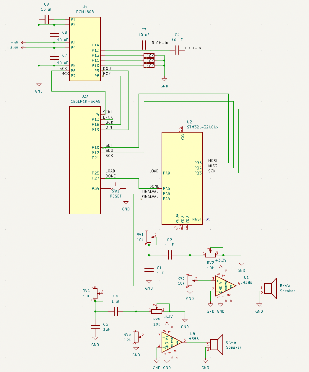
To read in the audio into the FPGA, we needed to use an Analog to Digital Converter (ADC) to convert analog stereo audio into digital data that our FPGA can manipulate. We opted to use the PCM1808, a 24-bit stereo ADC with I2S functionality. This goes beyond previous course material, as the PCM1808 uses I2S, a communication protocol we had yet to explore and made for audio. We passed in the two different audio channels into the left and right channels, with the FPGA acting as the controller. The wiring and block diagram between the FPGA and PCM1808 ADC is below, and outlines how the ADC interfaces with our system. Note that MD1, MD0, and FMT are set low with a pull-down resistor to set the PCM1808 as the worker with an I2S 24-bit data format.
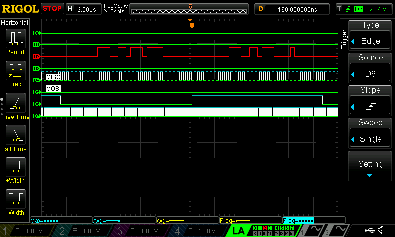
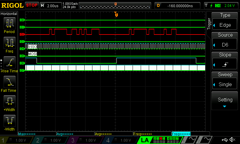
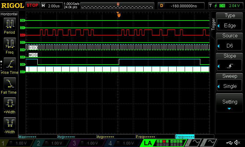
We confirm that the audio data is being read with I2S using a logic analyzer. Below are the traces for various audio gains, where D2 is connected to DOUT, D4 to BCK, D6 to LRCK, and D7 to SCKI. For this test, I set the clock to 12 MHz, therby setting the sampling frequency to be 46.875 kHz, as defined by the SCK. The Left/Right clock (LRCK) is set to 3 MHz, where 24 pulses from BCK occur every LRCK cycle. This is confirmed with the oscilloscope traces. The DOUT shows the digital output of the input audio signal. Since I2S encodes the amplitude into 24-bit values, we would expect lower volumes of music to have smaller 24-bit digital values. This behavior is demonstrated in the following traces, where as we decrease the volume, the MSB is lower and lower.

Digital Filtering
To apply digital filtering on the audio signal, we planned to utilize the MCU’s onboard ADC to read user inputs, use SPI to communicate EQ values between the MCU and FPGA, and generate the necessary FIR Coefficients.
We have set up the onboard MCU ADC to read in the four external potentiometer values and used SPI to transfer these EQ values to the FPGA to be used for digital filtering. We opted to use Finite Impulse Response (FIR) to apply low and high pass filters to the audio data. The EQ values correspond to 16 buckets between 0 to 20 kHz (the range of human hearing), with each bucket ranging 1.25 kHz (20 kHz/16). Thus, the EQ value would influence the passband and stopband of the filters. To implement FIR, we generated and tested the integer coefficients for the desired filters in Matlab and exported them as a .txt file. The filters have 128 taps, a number derived from preliminary testing to find the minimum number of taps needed to create the desired filters. The .txt file of coefficients is read into the FPGA using an FSM and similar logic as sbox_sync in lab 7. A block diagram of the system as implemented in ModelSim is shown below.
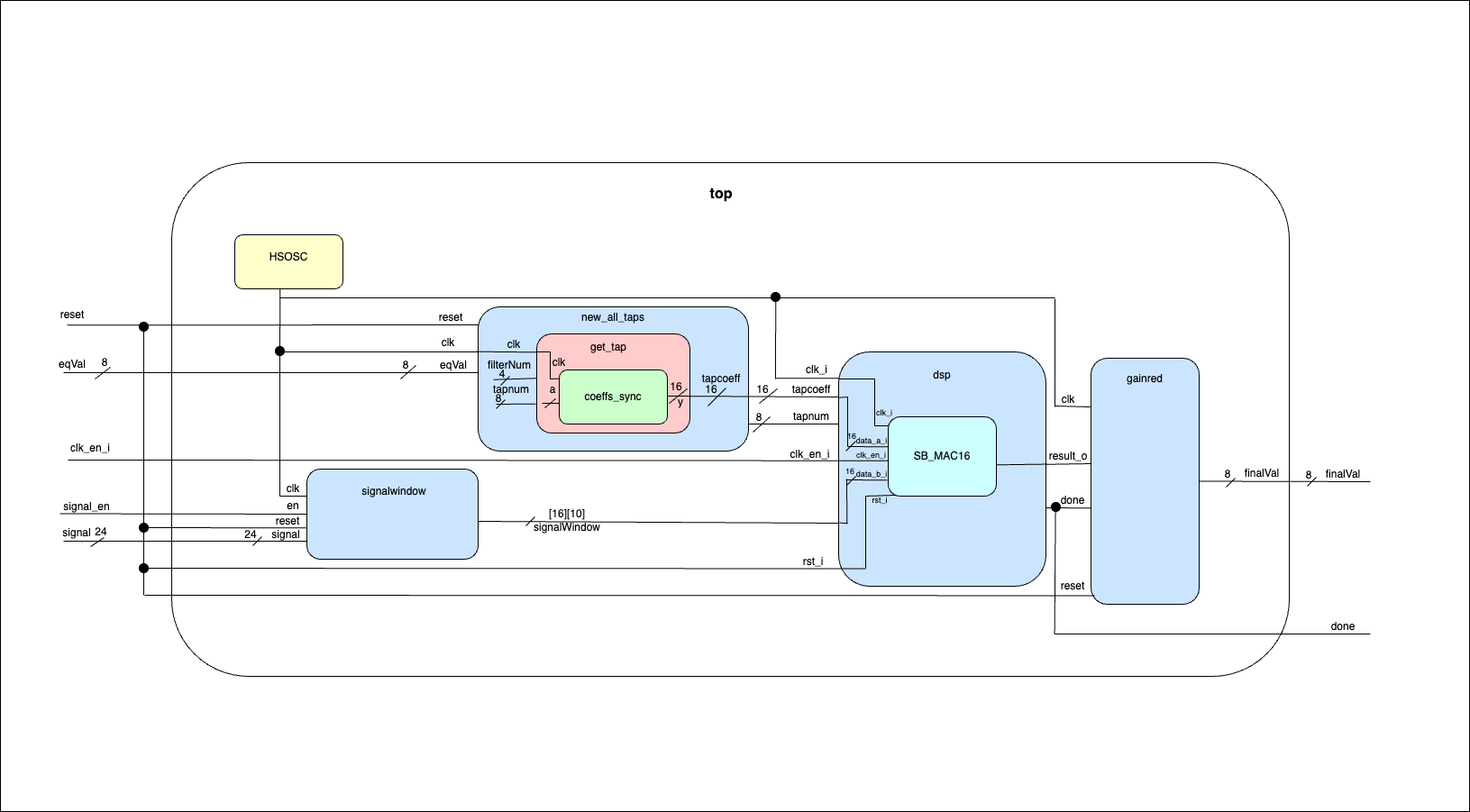
The EQ values are sent in from the MCU via SPI communication.
Generating Coefficients for FIR Filters
We opted to pass in FIR coefficients generated in MatLab so that we could utilize the DSP toolbox and easily visualize and adjust the filter and taps.
As a result, our Matlab script would generate the lowpass and highpass filter coefficients for the 16 EQ value buckets. and store these coefficients into a .txt file to be read by the FPGA.
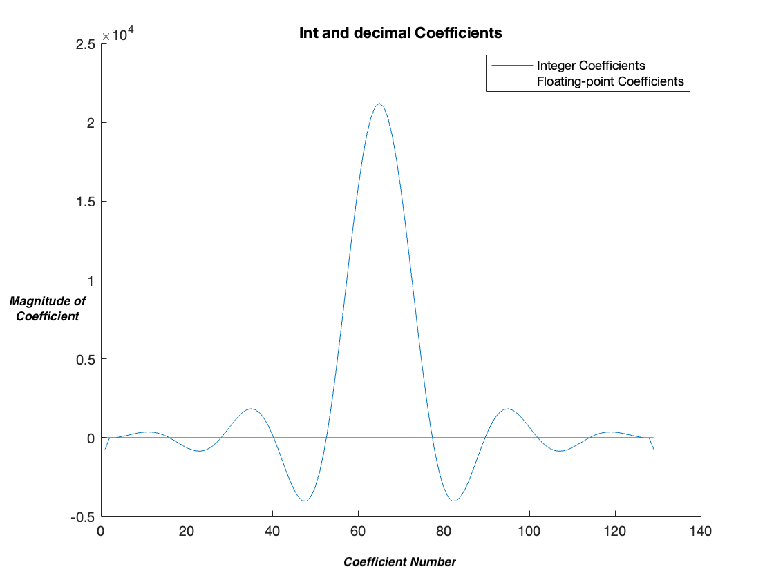
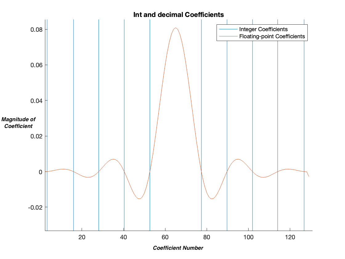
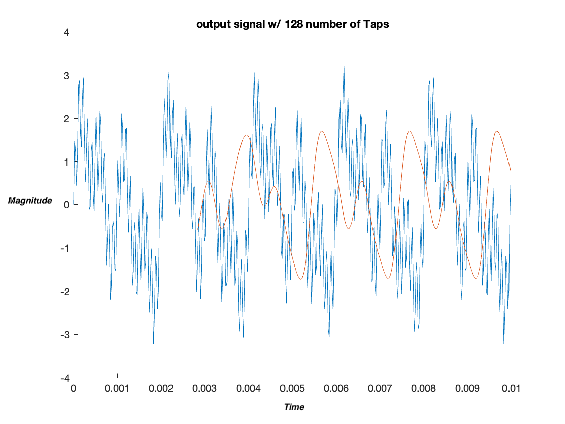
In order to use these coefficients in the FPGA, we wanted to convert the values from floating point to integer, which requires scaling the coefficients by a value of g. The floating point and integer coefficients are shown below, where if we scale the signal we see that the shape of the plots are the same. Thus, when plotting the output signal, it is critical to scale the signal by dividing by g. As there would only be 32 g values, we decided that we would hard code these values into the FPGA.
The below figures are for a lowpass filter with 128 taps and a pass band ending at 1250 hz.
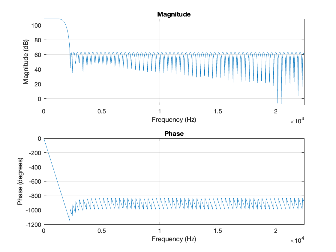
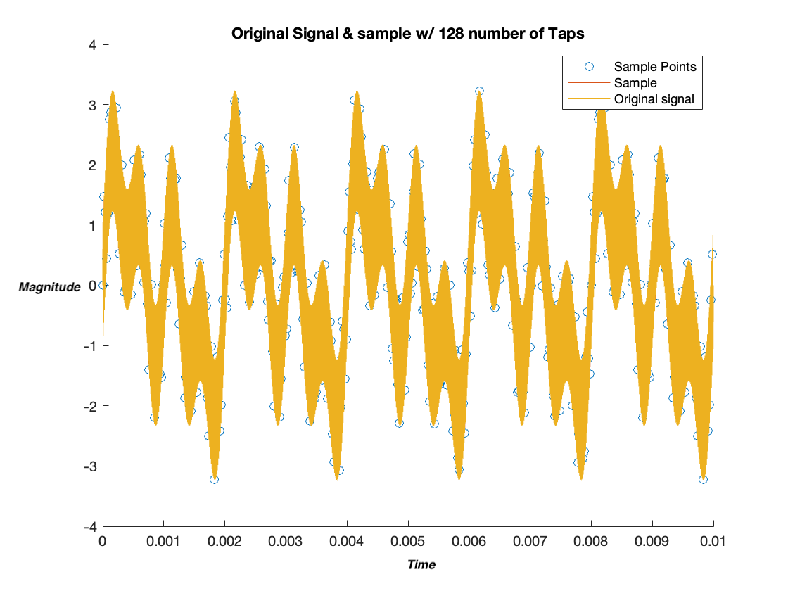
We then confirmed the design of these filters by creating a signal with multiple frequency components and applying our filter and gain scaling. To do this, we copied our verilog logic, allowing us to confirm that our logic acted as expected.
Passing in the Coefficients to the FPGA
In order to retrieve the proper coefficients, the filter number was input based on a digital input from the MCU. Thus, based on what the user selects, the code will then retrieve the set of 128 coefficients that correspond to the filter value that they requested. This was done by saving a .txt file with all 2048 coefficients (128 coefficients per filter, 16 different filter options), and then storing the desired coefficients synchronously in BRAM. An FSM is used to retrieve all 128 coefficients on each clock cycle that will then be used to digitally filter the signal.
Modeling DSP
The modules created in ModelSim contained code from Lab 7 to retrieve the different taps read from a .txt file stored in memory based on desired filter values received from the MCU via SPI. The FPGA would also create a signal window that would contain the past 10 samples of digital audio from the ADC to be used for FIR filtering. This signal window and the retrieved taps would then be input to the MAC to be multiplied and summed up together. The MAC was configured to take in 2 signed 16-bit inputs, and then output a 33-bit result for 10 tap coefficients. It also received the system clock as input generated from the high speed oscillator at 12 MHz. The output data from the MAC was then scaled back down by being divided by the filter’s gains, and then concatenated to 8 bits so that it could be sent out to the MCU via SPI.
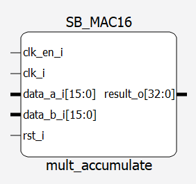

As shown in the images above, we got DSP to work in simulation, but did not succeed in implementing in hardware.
Outputting Audio
To output the audio to the MCU, the FPGA would wait for the audio data to be read in from the PCM1808. Once the entire sample was read, the left and right variables would be updated, and the Done flag would be raised. Then, the eq1_core module would pass the updated left channel audio data to the MCU. Once the left audio data was shifted out, the Done flag would be lowered. To learn more about the SPI handshake, see “FPGA and MCU Communication”